- 您现在的位置:买卖IC网 > Sheet目录346 > NCP5111DR2G (ON Semiconductor)IC DRIVER HI/LOW SIDE HV 8-SOIC
NCP5111
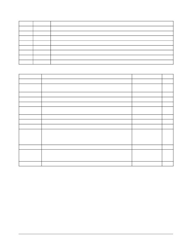
PIN DESCRIPTIONS
Pin No.
1
2
3
4
5
6
7
8
Pin Name
VCC
IN
GND
DRV_LO
NC
BRIDGE
DRV_HI
VBOOT
Pin Function
Low side and main power supply
Logic Input
Ground
Low side gate drive output
Not Connected
Bootstrap return or high side floating supply return
High side gate drive output
Bootstrap power supply
MAXIMUM RATINGS
Rating
V CC
V CC_transient
Symbol
Main power supply voltage
Main transient power supply voltage:
Value
? 0.3 to 20
23
Unit
V
V
IV CC_max = 5 mA during 10 ms
V BRIDGE
V BRIDGE
V BOOT ? V BRIDGE
V DRV_HI
V DRV_LO
dV BRIDGE /dt
V IN
VHV: High Voltage BRIDGE pin
Allowable Negative Bridge Pin Voltage for IN_LO Signal Propagation to DRV_LO
VHV: Floating supply voltage
VHV: High side output voltage
Low side output voltage
Allowable output slew rate
Inputs IN
? 1 to 600
? 10
? 0.3 to 20
V BRIDGE ? 0.3 to
V BOOT + 0.3
? 0.3 to V CC + 0.3
50
? 1.0 to V CC + 0.3
V
V
V
V
V
V/ns
V
ESD Capability:
? HBM model (all pins except pins 6 ? 7 ? 8)
? Machine model (all pins except pins 6 ? 7 ? 8)
Latchup capability per JEDEC JESD78
2
200
kV
V
R q JA
T J_max
Power dissipation and Thermal characteristics
PDIP ? 8: Thermal Resistance, Junction ? to ? Air
SO ? 8: Thermal Resistance, Junction ? to ? Air
Maximum Operating Junction Temperature
100
178
+150
° C/W
° C
Stresses exceeding Maximum Ratings may damage the device. Maximum Ratings are stress ratings only. Functional operation above the
Recommended Operating Conditions is not implied. Extended exposure to stresses above the Recommended Operating Conditions may affect
device reliability.
http://onsemi.com
3
发布紧急采购,3分钟左右您将得到回复。
相关PDF资料
NCP5304DR2G
IC DRIVER HI/LOW SIDE HV 8-SOIC
NCP5355DG
IC DRVR SYNC BUCK MOSF 12A 8SOIC
NCP5359ADR2G
IC MOSFET GATE DVR DUAL 8-SOIC
NCP5359DR2G
IC GATE DRIVER VR11.1/AMD 8-SOIC
NCP5360RMNR2G
IC DRIVER MOSFET 56QFN
NCP5366MNR2G
IC DRIVER MOSFET DFN
NCP5369MNR2G
IC DRIVER MOSFET DFN
NCP5623BMUTBG
IC LED DRIVER RGB I2C 12-LLGA
相关代理商/技术参数
NCP5111PG
功能描述:功率驱动器IC HIGH VOLT MOSFET DR MOSFET IGBT DRIVER RoHS:否 制造商:Micrel 产品:MOSFET Gate Drivers 类型:Low Cost High or Low Side MOSFET Driver 上升时间: 下降时间: 电源电压-最大:30 V 电源电压-最小:2.75 V 电源电流: 最大功率耗散: 最大工作温度:+ 85 C 安装风格:SMD/SMT 封装 / 箱体:SOIC-8 封装:Tube
NCP51190
制造商:ONSEMI 制造商全称:ON Semiconductor 功能描述:1.5A DDR Memory Termination Regulator
NCP51198PDR2G
功能描述:线性稳压器 - 标准 1.5A DDR Memory Termination Reg
RoHS:否 制造商:STMicroelectronics 输出类型: 极性: 输出电压:1.8 V 输出电流:150 mA 负载调节: 最大输入电压:5.5 V 线路调整率: 最大工作温度:+ 125 C 安装风格:SMD/SMT 封装 / 箱体:SOT-323-5L
NCP51199PDR2G
功能描述:线性稳压器 - 标准 DDR 2Amp Source Sink VTT Termination Reg
RoHS:否 制造商:STMicroelectronics 输出类型: 极性: 输出电压:1.8 V 输出电流:150 mA 负载调节: 最大输入电压:5.5 V 线路调整率: 最大工作温度:+ 125 C 安装风格:SMD/SMT 封装 / 箱体:SOT-323-5L
NCP511SN15T1
功能描述:低压差稳压器 - LDO 1.5V 150mA CMOS RoHS:否 制造商:Texas Instruments 最大输入电压:36 V 输出电压:1.4 V to 20.5 V 回动电压(最大值):307 mV 输出电流:1 A 负载调节:0.3 % 输出端数量: 输出类型:Fixed 最大工作温度:+ 125 C 安装风格:SMD/SMT 封装 / 箱体:VQFN-20
NCP511SN15T1G
功能描述:低压差稳压器 - LDO 1.5V 150mA CMOS w/Enable RoHS:否 制造商:Texas Instruments 最大输入电压:36 V 输出电压:1.4 V to 20.5 V 回动电压(最大值):307 mV 输出电流:1 A 负载调节:0.3 % 输出端数量: 输出类型:Fixed 最大工作温度:+ 125 C 安装风格:SMD/SMT 封装 / 箱体:VQFN-20
NCP511SN18T1
功能描述:低压差稳压器 - LDO 1.8V 150mA CMOS RoHS:否 制造商:Texas Instruments 最大输入电压:36 V 输出电压:1.4 V to 20.5 V 回动电压(最大值):307 mV 输出电流:1 A 负载调节:0.3 % 输出端数量: 输出类型:Fixed 最大工作温度:+ 125 C 安装风格:SMD/SMT 封装 / 箱体:VQFN-20
NCP511SN18T1G
功能描述:低压差稳压器 - LDO 1.8V 150mA CMOS w/Enable RoHS:否 制造商:Texas Instruments 最大输入电压:36 V 输出电压:1.4 V to 20.5 V 回动电压(最大值):307 mV 输出电流:1 A 负载调节:0.3 % 输出端数量: 输出类型:Fixed 最大工作温度:+ 125 C 安装风格:SMD/SMT 封装 / 箱体:VQFN-20
